Low-energy electron diffraction (LEED)
LEED is a experimental technique which is used to study the structure of (organic) adsorbates on metal
surfaces. The observed diffraction patterns allow for the determination of the unit cell size, its symmetry and
rotational alignment.
|
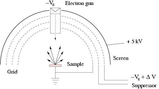 As depicted in the figure to the left,
electrons with typical energies between 20 - 200 eV are probing the surface structure. The elastic scattering
from surface region results in characteristic LEED patterns. As depicted in the figure to the left,
electrons with typical energies between 20 - 200 eV are probing the surface structure. The elastic scattering
from surface region results in characteristic LEED patterns.
In principle, the Ewald construction relates
those images to the 2-dimensional reciprocal lattice. More complicated LEED patterns, however, often require
(kinematical)
calculations in order to derive the symmetry of the adsorbate unit cell.
|
As adsorbate studies require clean surfaces, the LEED system is installed in an ultra-high vacuum system which is
suitable for the in situ characterization of monolayer films prepared by organic molecular
beam deposition.
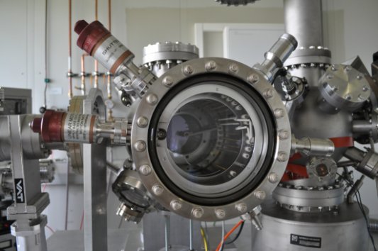
- The LEED system in our lab is an OCI BDL800IR-MCP with
two microchannel-plates which allow to use very small incident currents.
- A sensitive CCD camera can be installed to monitor the intensity on the fluorescence screen.
- The four-grid optic and an additional lock-in amplifier allow for Auger electron measurements.
- Picture of the LEED
electronics
|
|
|
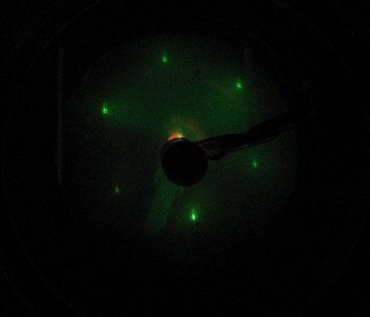 LEED pattern of a clean Cu(111) surface. This fcc
material shows the charateristic 3-fold symmetry. Note, that the (01) and (10) reflections are not
equivalent. LEED pattern of a clean Cu(111) surface. This fcc
material shows the charateristic 3-fold symmetry. Note, that the (01) and (10) reflections are not
equivalent.
|
For further information, see the LEED I(V) data
repository.
Recomended articles on the LEED technique:
[1] C. Davisson, L. H. Germer, Diffraction of Electrons by a Crystal of Nickel, Phys. Rev. 30
(1927) 705.
[2] M.A. Van Hove, W.H. Weinberg, C. M. Chan, Low-Energy Electron Diffraction Springer, Berlin
(1986).
[3] H. Lüth, Surfaces and Interfaces of Solids, Springer, Berlin (1993)