 Organic
semiconducting materials such as acenes, perylene-derivatives, and phthalocyanines are
presently receiving much attention due to their
attractive optical and structural properties. Several
spectacular phenomena and device applications have been demonstrated, such as diodes,
field-effect transistors up to all-organic integrated circuits, photodiodes, photovoltaic
cells, and light emitting diodes [1]. In fact, many of the devices and phenomena known from
inorganic semiconductors, which are determining much present-day technology, have been
realized with organics, and we are presently facing what may be called a "molecular
electronics revolution".
Organic
semiconducting materials such as acenes, perylene-derivatives, and phthalocyanines are
presently receiving much attention due to their
attractive optical and structural properties. Several
spectacular phenomena and device applications have been demonstrated, such as diodes,
field-effect transistors up to all-organic integrated circuits, photodiodes, photovoltaic
cells, and light emitting diodes [1]. In fact, many of the devices and phenomena known from
inorganic semiconductors, which are determining much present-day technology, have been
realized with organics, and we are presently facing what may be called a "molecular
electronics revolution".
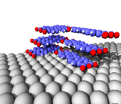
While it is clear that for certain applications like high-speed electronics inorganic materials are superior in terms of performance (due to their higher charge carrier mobility), organic materials can have advantages in certain other respects [2]. One of the attractive features of organics is the potential tunability of their functional properties by means of chemical synthesis. For instance, the emission colour in optoelectronic devices can be tuned by attaching or replacing a certain functional group while leaving the "core" of the molecule unchanged. New and different parameter ranges, e.g., for the effective mass of the charge carriers and the dielectric function and, thus, new areas of physics, are accessible.
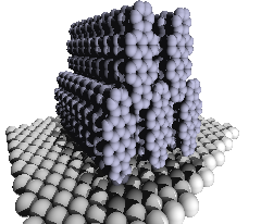
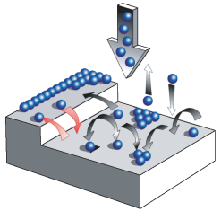 For device
applications, it is generally agreed that the use of single crystals is less practical, and
consequently much effort is devoted to the growth of highly ordered thin films [4]. To this
end, organic molecular beam deposition (OMBD) holds the promise for optimum control of the
structure and purity. Yet, there are several challenges to face, which are both of practical
relevance and of fundamental interest:
For device
applications, it is generally agreed that the use of single crystals is less practical, and
consequently much effort is devoted to the growth of highly ordered thin films [4]. To this
end, organic molecular beam deposition (OMBD) holds the promise for optimum control of the
structure and purity. Yet, there are several challenges to face, which are both of practical
relevance and of fundamental interest: