 Smilar to conventional (inorganic)
semiconductors, organic semiconductors can be used for
devices such as organic photovoltaics (OPV).
While the charge carrier mobility and the photovoltaic
efficiency is not assumed to rival that of, silicon-based
photovoltaics, the idea for OPV is to produce OPV cells at
lower cost and in particular lower energy consumption than for
silicon.
Another important issue is that organic devices may be made
mechanically flexible and thinner than silicon (thanks to
their higher optical absorption, i.e. stronger transitions),
which potentially opens up completely new applications not
possible with silicon technology, such as OPV on clothes, e.g.
In order to optimise and use these systems in applications,
research is required to understand the fundamental mechanisms
underlying OPV. This is the subject of a focus program funded
by the DFG, in which are participating.
Smilar to conventional (inorganic)
semiconductors, organic semiconductors can be used for
devices such as organic photovoltaics (OPV).
While the charge carrier mobility and the photovoltaic
efficiency is not assumed to rival that of, silicon-based
photovoltaics, the idea for OPV is to produce OPV cells at
lower cost and in particular lower energy consumption than for
silicon.
Another important issue is that organic devices may be made
mechanically flexible and thinner than silicon (thanks to
their higher optical absorption, i.e. stronger transitions),
which potentially opens up completely new applications not
possible with silicon technology, such as OPV on clothes, e.g.
In order to optimise and use these systems in applications,
research is required to understand the fundamental mechanisms
underlying OPV. This is the subject of a focus program funded
by the DFG, in which are participating.
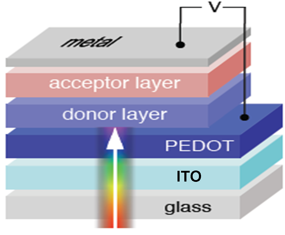
Organic solar cells basically consist of an organic
semiconductor in contact with two metal electrodes, which
collect the charge carriers produced in the semiconductor upon
light irradiation. In order to illuminate the semiconductor
material at least one of the two electrodes has to be
transparent. Glass or plastic substrates coated with ITO
(indium tin oxide, a conductive oxide with low resistivity,
high transparency in the visible and a relatively high work
function [1]) are commonly used for this purpose.
On top of the ITO a buffer layer may be deposited. The most
common material used is the polymer blend PEDOT:PSS, an
organic conducting material with relatively good
electrochemical, ambient and thermal stability. Moreover, the
electrical properties of PEDOT:PSS can be varied by changing
the mixing ratio of the blend [2]. The reported benefits of
PEDOT:PSS films between the ITO and the photovoltaic active
layer are:
- preventing indium diffusion in the semiconductors
- improving the compatibility between the energy levels of the organic semiconductors with the work function of the electrode [3].
 In order to collect the photo-generated charges
the second metallic contact (e.g. Al, Ag) is deposited on top
of the active material.
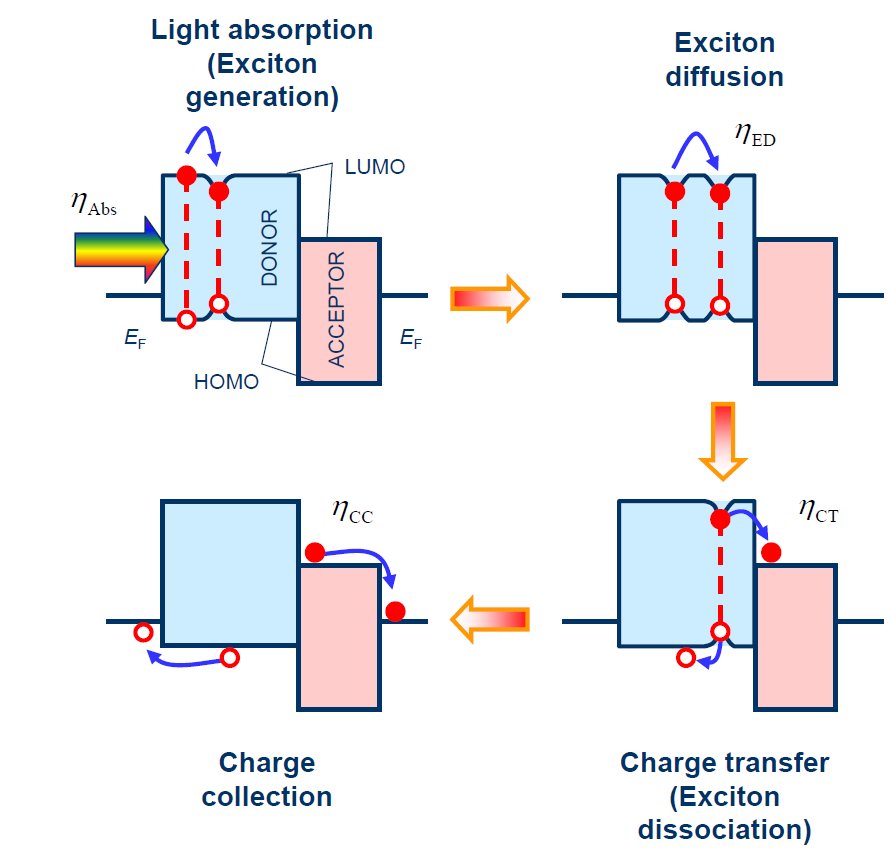
The photo-active layer usually consists of a hetero-junction
formed by two different semiconductors, i.e. an electron-donor
(D) and an electron-acceptor (A) material. Donor molecules
exhibit a low ionization potential (high HOMO energy), while
acceptor molecules have a high electron affinity (low LUMO
energy). Visible light may excite electrons from the HOMO to
the LUMO level, therefore leaving a hole in the HOMO
level. The relatively low dielectric constant in organic
materials leads to the formation of a neutral bound
electron-hole pair, known as exciton.
The organic semiconductors have to be chosen properly for the
hetero-junction, so that the electronic band structure of the
donor and acceptor materials is matched. The different
alignment of the HOMO and LUMO levels allows for exciton
dissociation at the interface. Electrons are then transferred
through the acceptor and collected by the electrode (Al),
while the respective holes diffuse in the acceptor and then in
the ITO electrode.
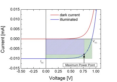
To determine the electric behaviour of a solar cell the
current-vs-voltage characteristic is measured. One may
distinguish different regimes:
In order to collect the photo-generated charges
the second metallic contact (e.g. Al, Ag) is deposited on top
of the active material.
The photo-active layer usually consists of a hetero-junction
formed by two different semiconductors, i.e. an electron-donor
(D) and an electron-acceptor (A) material. Donor molecules
exhibit a low ionization potential (high HOMO energy), while
acceptor molecules have a high electron affinity (low LUMO
energy). Visible light may excite electrons from the HOMO to
the LUMO level, therefore leaving a hole in the HOMO
level. The relatively low dielectric constant in organic
materials leads to the formation of a neutral bound
electron-hole pair, known as exciton.
The organic semiconductors have to be chosen properly for the
hetero-junction, so that the electronic band structure of the
donor and acceptor materials is matched. The different
alignment of the HOMO and LUMO levels allows for exciton
dissociation at the interface. Electrons are then transferred
through the acceptor and collected by the electrode (Al),
while the respective holes diffuse in the acceptor and then in
the ITO electrode.
To determine the electric behaviour of a solar cell the
current-vs-voltage characteristic is measured. One may
distinguish different regimes:
- If no external voltage is applied, no current flows through the junction.
- If an external voltage is applied under reverse bias, a current flux is possible.
- If an external voltage is applied in forward bias condition, current flow is allowed.
Upon illumination, the device will act as a current generator, therefore the I-V curve shifts downward, as illustrated in the figure below.
 In order to produce such devices on a
conducting transparent substrate, the photo-active materials
have to be deposited. Two main types of techniques are
available:
In order to produce such devices on a
conducting transparent substrate, the photo-active materials
have to be deposited. Two main types of techniques are
available: